
Quantum Computing
Project Summary
Quantum computing? Cool! The idea of quantum computing is that instead of performing calculations using a series of two states (1’s and 0’s, called ‘bits’), we can use quantum objects that can have a multiple states (more appropriately, a superposition of states, called ‘qubits’). Having this capability would allow for very fast computations on enormous datasets. There are, in fact, many methods to making a quantum computer. One such type of quantum computer is called a topological quantum computer. This type of quantum computer works by utilizing theoretical predicted 2-dimensional quasiparticles called ‘anyons’.
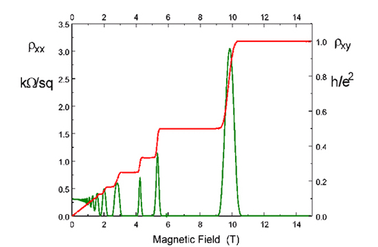
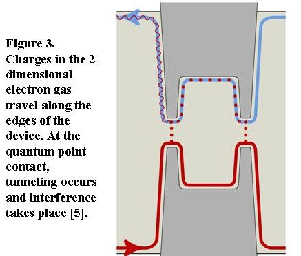
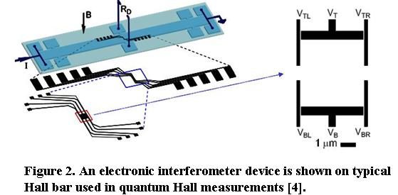
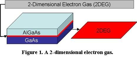
The details of what these particles are and how they work in a topological quantum computer are complicated. However, my work at Harvard University in Professor Charles Marcus’ group was fabricating nanodevices and testing those devices to try and identify the experimentally elusive anyon. The devices used were electronic Fabry-Perot interferometers which were fabricated on high mobility Gallium Arsenide / Aluminum Gallium Arsenide heterostructures. These devices had been successfully used in the integer quantum Hall regime, but lacked the electrostatic stability needed for interference measurements at fractional filling factors. This is likely due to the fact that the doping of the material is optimized for high mobility, leading to poor gateability. During this research, we developed of a new generation of devices where gates were deposited in etched trenches rather than on the surface of the chip, allowing them to operate at smaller voltages where they are more stable. Even though the etched gate allowed for a decrease of 0.3 V to deplete the 2-dimensional electron gas at the GaAs/AlGaAs interface, the device was still not able to resolve the fractional filling factor.
Related Media
Publications
Published
- Roder P. “Fabrication of a Stable Tunable Electronic Fabry-Perot Interferometer in the Fractional Quantum Hall Regime.” 2009 NNIN REU Research Accomplishments, 134-135, (2009).
Acquired Skills
Device Nanofabrication
CAD Device Design
Wafer Cleaning & Dicing
Wafer Resist Spinning & Developing
Electron Beam Lithography
Wafer Acid Etching & Profilometry
Thermal & Electron Beam Metal Deposition
Device Characterization
Wire Bonding
Low Temperature & High Magnetic Field I-V Testing
SEM Inspection
Research Lab
Location
Harvard University, Physics
Lab PI
Research Mentors
Dr. Angela Kou
Dr. Douglas McClure